
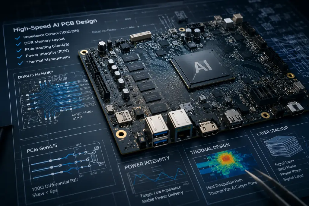
AI hardware is becoming more powerful, but also more demanding at the PCB and PCBA level. High-speed AI workloads often involve fast processors, DDR memory, PCIe interfaces, high-current power rails, dense BGA packages, and continuous thermal stress.
For AI cameras, edge computing devices, industrial vision systems, robotics controllers, and embedded AI platforms, a stable PCB design is just as important as the AI chip itself. Poor signal integrity, weak power delivery, or insufficient heat dissipation can cause system crashes, data errors, reduced inference speed, or long-term reliability issues.
This guide covers key PCBA design practices for high-speed AI hardware projects.
1. Start with Signal Integrity Planning
High-speed AI systems usually include interfaces such as DDR, PCIe, MIPI, USB 3.0, Ethernet, HDMI, or high-speed sensor inputs. These signals cannot be routed like ordinary low-speed traces.
For high-speed digital signals, controlled impedance is important. Many designs use 50ω single-ended impedance or 100ω differential impedance, depending on the interface requirements.
To maintain stable impedance, engineers need to control:
- Trace width
- Trace spacing
- Copper thickness
- Dielectric thickness
- PCB material
- Reference plane continuity
- Via structure
- Layer stack-up
Impedance mismatch can cause signal reflection, timing errors, and unstable data transmission. This becomes more serious as signal frequency increases.
Before PCB fabrication, it is recommended to confirm the stack-up with the PCB manufacturer and to run impedance calculations or simulations as needed.
2. Keep Reference Planes Continuous
A high-speed signal trace needs a clear return path. If the reference plane is split or interrupted, the return current must find another path. This can increase noise, EMI, and signal distortion.
For AI hardware boards, this is especially important around DDR memory, PCIe lanes, camera interfaces, and high-speed connectors.
Good practices include:
- Avoid routing high-speed signals across split planes
- Keep ground reference continuous under critical traces
- Use ground stitching vias near layer transitions
- Avoid unnecessary gaps in reference planes
- Separate noisy power areas from sensitive signal areas
Stable reference planes help improve signal integrity and reduce EMI risk.
3. DDR Memory Layout Requires Careful Control
DDR memory is one of the most sensitive parts of many AI hardware designs. AI processors often depend on high memory bandwidth, so DDR layout quality directly affects system performance and stability.
DDR3, DDR4, and DDR5 interfaces have strict timing requirements. Data, address, command, and clock signals must be routed in accordance with the chip vendor’s layout guidelines.
Important points include:
- Length matching for related signal groups
- Controlled impedance routing
- Proper spacing between signal groups
- Clean reference planes
- Short and direct routing where possible
- Careful clock signal protection
- Correct termination and decoupling design
The exact length-matching tolerance should follow the memory controller and DDR chip datasheets. Instead of using one fixed value for every project, engineers should confirm requirements based on the selected processor, memory type, PCB stack-up, and operating speed.
For production, DDR-related failures can be difficult to debug. Early layout review is strongly recommended before fabrication.
4. PCIe Routing Needs Strict Differential Pair Control
PCIe is common in AI hardware because many systems use AI accelerator cards, high-speed storage, wireless modules, or expansion interfaces.
PCIe Gen3, Gen4, and Gen5 signals require strict differential pair routing. The higher the generation, the more sensitive the design becomes.
Key layout points include:
- Maintain 100Ω differential impedance
- Keep pair-to-pair spacing sufficient
- Match length within each differential pair
- Reduce vias where possible
- Avoid routing over split reference planes
- Keep connectors and AC coupling capacitors placed correctly
- Follow the chip and connector vendor layout guide
Vias, stubs, sharp bends, poor connectors, and reference plane discontinuity can all reduce PCIe signal quality.
For high-speed PCIe projects, simulation and careful connector selection are recommended.
5. Power Integrity Is Critical for AI Chips
AI processors, GPUs, NPUs, and FPGAs often require low-voltage, high-current power rails. Some core voltages may be below 1V while drawing very high current during peak inference workloads.
This creates a serious power integrity challenge. If the power distribution network is not well designed, voltage drop or transient noise may cause resets, unstable operation, or reduced performance.
Important design practices include:
- Use dedicated power and ground planes
- Place decoupling capacitors close to power pins
- Use multiple capacitor values for different frequency ranges
- Keep high-current paths short and wide
- Use enough vias for current transfer between layers
- Separate noisy switching power areas from sensitive circuits
- Check voltage drop and current density
- Validate the design under real load conditions
For AI workload testing, average power is not enough. The design should also handle sudden changes in current during model inference.
6. Thermal Design Should Start Early
High-performance AI chips can generate significant heat. If thermal design is considered too late, the final product may suffer from thermal throttling, unstable performance, or shortened component life.
Thermal planning should begin during PCB layout and mechanical design.
Useful practices include:
- Use thermal vias under heat-generating components
- Connect thermal pads to the inner or bottom copper layers
- Reserve mounting space for heatsinks
- Consider the airflow path and enclosure design
- Avoid placing heat-sensitive components near hot chips
- Use copper areas to spread heat
- Run thermal simulation for high-power designs
- Test temperature during continuous AI workload operation
For edge AI devices, thermal design is often more difficult because the enclosure is compact and fanless operation may be required.
7. BGA Fanout and Assembly Reliability Matter
Many AI chips, FPGAs, and memory devices use fine-pitch BGA packages. These packages require careful PCB layout and reliable SMT assembly control.
Designers should consider:
- BGA pitch and routing feasibility
- Via-in-pad requirements
- HDI stack-up if needed
- Solder mask design
- X-ray inspection requirements
- Rework difficulty
- Warpage control
- PCB thickness and rigidity
For high-density AI boards, DFM review before production can help reduce assembly defects and avoid layout changes later.
8. Plan for Testing Before Production
Testing should not be treated as an afterthought. A board may pass visual inspection but still fail under real AI workloads.
For high-speed AI PCBA projects, testing may include:
- AOI inspection
- X-ray inspection for BGA solder joints
- ICT testing where applicable
- Power-on testing
- Firmware programming
- DDR memory testing
- PCIe link testing
- Thermal stress testing
- Functional AI workload testing
Adding test points early can make production testing and debugging much easier.
If test access is missing, even a small problem can take much longer to find during batch production.
9. BOM and Component Availability Should Be Reviewed Early
High-speed AI boards often depend on advanced processors, DDR memory, power ICs, connectors, oscillators, and communication modules. Some of these parts may have long lead times or limited supply.
Before moving into production, hardware teams should review:
- Main chip availability
- Alternative memory options
- Power IC supply stability
- Connector compatibility
- EOL risk
- MOQ requirements
- Lead time
- Programming and testing tools
A good BOM review can reduce production delays and help control total project cost.
Conclusion
High-speed AI PCBA design is not only about routing fast signals. It requires a balanced design covering signal integrity, power integrity, thermal management, layout manufacturability, component sourcing, and production testing.
For AI hardware teams, the best time to solve these issues is before fabrication and assembly. Early DFM review, BOM checking, stack-up confirmation, and test planning can reduce risk when moving from prototype to small-batch or volume production.
PCBAEng supports high-speed AI hardware projects with PCB assembly, component sourcing, DFM review, SMT assembly, BGA inspection, testing support, and prototype-to-production manufacturing.